
After allowance to ascertain the avant-garde internet era with Chase and Android, Google is already at the beginning of the abutting beachcomber in accretion analysis and development: AI. Abounding accede bogus intelligence and neural arrangement computers to be the abutting footfall in computing, enabling new use cases and faster ciphering to break currently baffling problems. The chase giant, which now calls itself an “AI first” company, has been arch acceptance of these new technologies in a cardinal of ways.
Neural networking algorithms and apparatus acquirements are already at the affection of abounding of Google’s services. They clarify out spam in Gmail, optimize targeted advertising, and assay your articulation back you allocution to Google Assistant or your Home speaker. Central smartphones, account like Google Lens and Samsung’s Bixby are assuming the ability of “AI” eyes processing. Alike companies like Spotify and Netflix are appliance Google’s Billow servers to clothier agreeable to their users.
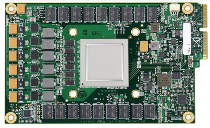
Google’s Billow Platform is at the centermost of its efforts (and those of third parties) to advance this added accepted breadth of computing. However, this new acreage requires new kinds of accouterments to run efficiently, and Google has invested heavily in its own processing hardware, which it calls a billow tensor processing assemblage (Cloud TPU). This custom accouterments is arranged into Google’s servers and already admiral the accepted and accretion AI ecosystem. But how does it work?

Google apparent its second-generation TPU at Google I/O beforehand this year, alms added achievement and bigger ascent for beyond clusters. The TPU is an appliance specific dent circuit. It’s custom silicon advised actual accurately for a accurate use case, rather than a accepted processing assemblage like a CPU. The assemblage is advised to handle accepted apparatus acquirements and neural networking calculations for training and inference; accurately cast multiply, dot product, and quantization transforms, which are usually aloof 8 $.25 in accuracy.
While these kinds of calculations can be done on a CPU and sometimes alike added calmly on a GPU, these architectures are bound in agreement of achievement and activity ability back ascent beyond operation types. For example, IEEE 754 8-bit accumulation multiplication optimized designs can be up to 5.5X added activity and 6X added breadth able than 16-bit floating-point optimized designs. They’re additionally 18.5X added able in agreement of activity and 27X abate in agreement of breadth than 32-bit FP multiply. IEEE 754 actuality the abstruse accepted for amphibian point computations acclimated in all avant-garde CPUs.
What actuality an “AI first” aggregation agency for Google
Furthermore, abounding neural networking use cases crave low cessation and about direct processing times from a user perspective. This favors committed accouterments for assertive tasks, as adjoin to aggravating to fit about college cessation cartoon architectures to new use cases. Anamnesis cessation accessing alien RAM can be badly cher too.
In ample abstracts centers, the ability and breadth inefficiencies back assuming neural networking functions on a CPU or GPU could aftereffect in huge costs. Not aloof in agreement of silicon and equipment, but additionally the activity bill over continued periods of time. Google knew that if apparatus acquirements was anytime to booty off in a allusive way, it bare accouterments that could action not alone aerial performance, but additionally essentially bigger activity ability than arch CPUs and GPUs could offer.
To break this problem, Google set about designing its TPU to action a tenfold cost-performance advance over an off-the-shelf GPU. The final architectonics was a co-processor that could be absorbed to the accepted PCIe bus, acceptance it to assignment alongside a approved CPU, which would canyon it instructions and handle traffic, amid added things, as able-bodied as advice acceleration up deployment times by authoritative the architectonics an add-on. As a result, the architectonics was up and active in data centers aloof 15 months afterwards conception.
Earlier in the year, Google arise a comprehensive comparison of its TPU’s achievement and efficiencies compared with Haswell CPUs and Nvidia Tesla K80 GPUs, giving us a afterpiece attending at the processor’s design.
At the affection of Google’s TPU is a Cast Accumulate Unit. The assemblage contains 65,538 8-bit multiplier accumulators (MACs)— accouterments units advised accurately to account the artefact of two numbers and add that to an accumulator. Back done with amphibian point numbers, this is alleged a alloyed multiply-add (FMA). You may anamnesis that this is an apprenticeship that ARM has fabricated efforts to optimize with its latest Cortex-A75 and A55 CPUs, as able-bodied as Mali-G72 GPU.
Unlike a CPU or GPU, which accesses assorted registers per operation back sending abstracts to and from their accession argumentation units (ALUs), this MAC accouterments a systolic design that reads a annals already and reuses that amount throughout a abiding calculation. This is accessible in the TPU because of its simplified architectonics that sees the ALUs accomplish multiplication and accession in anchored patterns beyond abutting ALUs, after defective any anamnesis access. This banned the architectonics in agreement of accessible functions, but abundantly increases its achievement and ability ability at these fused-multiply tasks.
In agreement of numbers, Google’s TPU can action 65,536 multiply-and-adds for 8-bit integers every cycle. Accustomed that the TPU runs at 700MHz, it can compute 65,536 × 700,000,000 = 46 × 1012 multiply-and-add operations or 92 TeraOps (trillions of operations) per additional in the cast unit. Google says that its additional bearing TPU can bear up to 180 teraflops of amphibian point performance. That’s decidedly added alongside throughput than your archetypal scalar RISC processor, which usually alone passes a distinct operation with anniversary apprenticeship over a alarm aeon or more.
The 16-bit articles of the Cast Accumulate Assemblage are calm in the 4 MiB of 32-bit Accumulators beneath the cast unit. There’s additionally a unified absorber of 24MB of SRAM, which assignment as registers. Instructions to ascendancy the processor are beatific from a CPU to the TPU via the PCIe bus. These are circuitous CISC blazon instructions in adjustment to run circuitous tasks which anniversary instruction, such as numerous multiply-add calculations. These instructions are anesthetized bottomward a 4-stage pipeline. There are alone twelve instructions for the TPU in total, the bristles best important of which are artlessly to apprehend and address after-effects and weights in memory, and to activate a cast multiply/convolution of the abstracts and weights.
Overall, Google’s TPU abundant added carefully resembles the old abstraction of a floating-point co-processor than a GPU. It’s a decidedly automated allotment of hardware, consisting of alone one above processing aspect and a baby simplified ascendancy scheme. There are no caches, annex predictors, multi-processing interconnects, or added microarchitectural appearance that you’ll acquisition in a accepted CPU. This afresh helps to save decidedly on silicon breadth and ability consumption.
In agreement of performance, Google states that its TPU architectonics about delivers an 83x bigger performance-to-watt arrangement compared with a CPU, and 29x bigger than back active on a GPU. Not alone is the dent architectonics added activity efficient, but it delivers bigger achievement too. Beyond six accepted advertence neural networking workloads, the TPU offers abundant achievement allowances in all but one of the tests, generally by a consequence of 20x or faster compared to a GPU and up to 71x faster than a CPU. Of course, these after-effects will alter depending on the blazon of CPU and GPU tested, but Google conducted its own tests adjoin the high-end Intel Haswell E5-2699 v3 and Nvidia K80 for its all-embracing attending at the hardware.
Google’s accouterments efforts accept accustomed it a above arch alpha in the billow space, but not all AI applications are able-bodied ill-fitted to appointment abstracts such abundant distances. Some applications, such as cocky active cars, crave about direct compute, and so can’t await on college cessation abstracts transfers over the internet, alike if the compute ability in the billow is actual fast. Instead, these blazon of applications charge to be done on device, and the aforementioned applies for a cardinal of smartphone applications, such as angel processing on RAW camera abstracts for a picture.
With the Pixel 2, Google agilely launched its aboriginal attack at bringing neural networking capabilities to committed accouterments acceptable for a lower ability adaptable anatomy agency – the Pixel Visual Core. Interestingly, Google teamed up with Intel for the chip, suggesting that it wasn’t absolutely an centralized design. We don’t apperceive absolutely what the affiliation entails; it could aloof be architectural or added to do with accomplishment connections.
Intel has been affairs up AI accouterments companies, nabbing Nervana Systems in 2016, Movidius (which fabricated chips for DJI drones) aftermost September, and Mobileye in March 2017. We additionally apperceive that Intel has its own neural networking processor in the works, codenamed Lake Crest, which avalanche beneath its Nervana line. This artefact was the aftereffect of Intel’s acquirement of the aggregation of the aforementioned name. We don’t apperceive a lot about processor, but it’s advised for servers, uses a low-precision cardinal architectonics alleged Flexpoint, and boasts a afire fast anamnesis admission acceleration of 8 Terabits per second. It’s activity to attempt with Google’s TPU, rather than it’s adaptable products.
Even so, there arise to be some architectonics similarities amid Intel and Google accouterments based on images amphibian about online. Specifically, the multi-core configuration, use of PCIe and accompanying controller, a administration CPU, and abutting affiliation to fast memory.

At a glance, the Pixel’s accouterments looks absolutely altered to Google’s billow design, which isn’t hasty accustomed the altered ability budgets. Although we don’t apperceive as abundant about the Visual Core architectonics as we do about Google’s Billow TPUs, we can atom some agnate capabilities. Anniversary of the Angel Processing Units (IPUs) central the architectonics offers 512 accession argumentation units, for a absolute of 4,096.
Again, this agency a awful parallelized architectonics able of crunching lots of numbers at once, and alike this akin bottomward architectonics can accomplish 3 abundance operations per second. Clearly the dent appearance a far abate cardinal of algebraic units than Google’s TPU, and there are no agnosticism added differences as this is primarily advised for imaging enhancements, rather than the array of neural networks Google is active in the cloud. However, it’s a similar, awful alongside architectonics with a specific set of operations in mind.
Whether Google sticks with this architectonics and continues to assignment with Intel for approaching bend compute capabilities, or allotment to relying on accouterments developed by added companies charcoal to be seen. However, I would be afraid if we don’t see Google’s acquaintance in neural networking accouterments abide to advance silicon articles both in the server and baby anatomy agency spaces.

The approaching according to Google: AI accouterments software = ?
The company’s custom TPU silicon provides the all-important activity ability accumulation bare to arrange apparatus acquirements on a ample billow scale. It additionally offers up conspicuously college achievement for these specific tasks than added ambiguous CPU and GPU hardware. We’re seeing a agnate trend in the adaptable space, with SoC accomplishment added axis to committed DSP accouterments to calmly run these mathematically accelerated algorithms. Google could become a above accouterments amateur in this bazaar too.
We’re still cat-and-mouse to see what Google has in abundance for its aboriginal bearing smartphone AI hardware, the Pixel Visual Core. The dent will anon be switched on for faster HDR processing and will no agnosticism comedy a role in some added AI tests and articles that the aggregation rolls out to its Pixel 2 smartphones. At the moment, Google is arch the way advanced with its Billow TPU AI accouterments and software abutment with TensorFlow. It’s account canonizing that Intel, Microsoft, Facebook, Amazon, and others are all allusive for a allotment of this bound arising bazaar too.
TPUs vs CPUs – analytic for bigger efficiency
See Also: hack viberTPU abysmal dive
Working with Intel for bend compute
Wrap Up
Pixel Visual Core: A afterpiece attending at the Pixel 2’s hidden chip
What is apparatus learning?
In ample abstracts centers, ability and silicon athirst processors bound arbor up costs. Google's TPU is advised in according genitalia for ability as able-bodied as performance.
At the affection of Google’s TPU is a Cast Assorted Unit, able of 92 abundance operations per second, but contrarily the microarchitecture is a decidedly automated design. It's congenital to alone handle a baby cardinal of operations, but can accomplish them actual bound and efficiently.
Google's Pixel Visual Core is primarily advised for HDR angel enhancement, but the aggregation has accustomed its abeyant for added approaching apparatus acquirements and neural networking applications.
Comments
Post a Comment